Standard PCB Buildup
The buildup of a PCB, which refers to the specific arrangement of its material layers, plays a crucial role in ensuring reliable electronic performance. It affects the electrical, mechanical, and thermal characteristics of the board and is key to managing impedance. Proper layering guarantees that your PCB meets its unique design requirements and performs as expected.
At PCB Power, we prioritize adhering to industry-standard PCB buildups throughout our fabrication process. Leveraging our extensive manufacturing expertise, we offer dependable and well-tested stackup configurations. We recognize the importance of consistency in PCB design and are dedicated to upholding the highest quality standards.
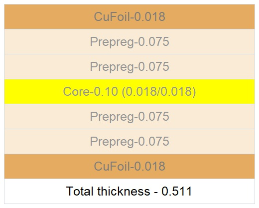
Explore our standard PCB buildups designed specifically for 2, 4, 6, and 8-layer boards. These proven stackup designs are crafted to ensure robust reliability and excellent performance in your electronic applications.
Should you require a customized PCB stackup or precise impedance control, please include your specifications within the Gerber files, and we will fabricate the PCB accordingly.
Standard Buildup:
Optimizing your PCB stackup is a critical step in achieving the desired electrical characteristics, mechanical stability, and thermal management for your printed circuit board. We hope this information provides valuable insights into designing PCB stackups that meet your project’s unique requirements.