Impedance Controlled Standard Build-Ups
Impedance-controlled buildups refer to precisely designed PCB layer stacks that maintain accurate electrical impedance to ensure the integrity of signals in high-frequency circuits. Such control is essential in today’s advanced PCB design to minimize signal degradation and interference, especially in complex multilayer boards.
At pcbxpress, we specialize in delivering industry-compliant impedance-controlled stackups for PCB manufacturing. Backed by deep experience in PCB fabrication, we provide dependable, finely tuned stack-up solutions that satisfy strict signal integrity standards. We understand the importance of consistent impedance in achieving high-performance PCB designs and are dedicated to maintaining top quality and reliability.
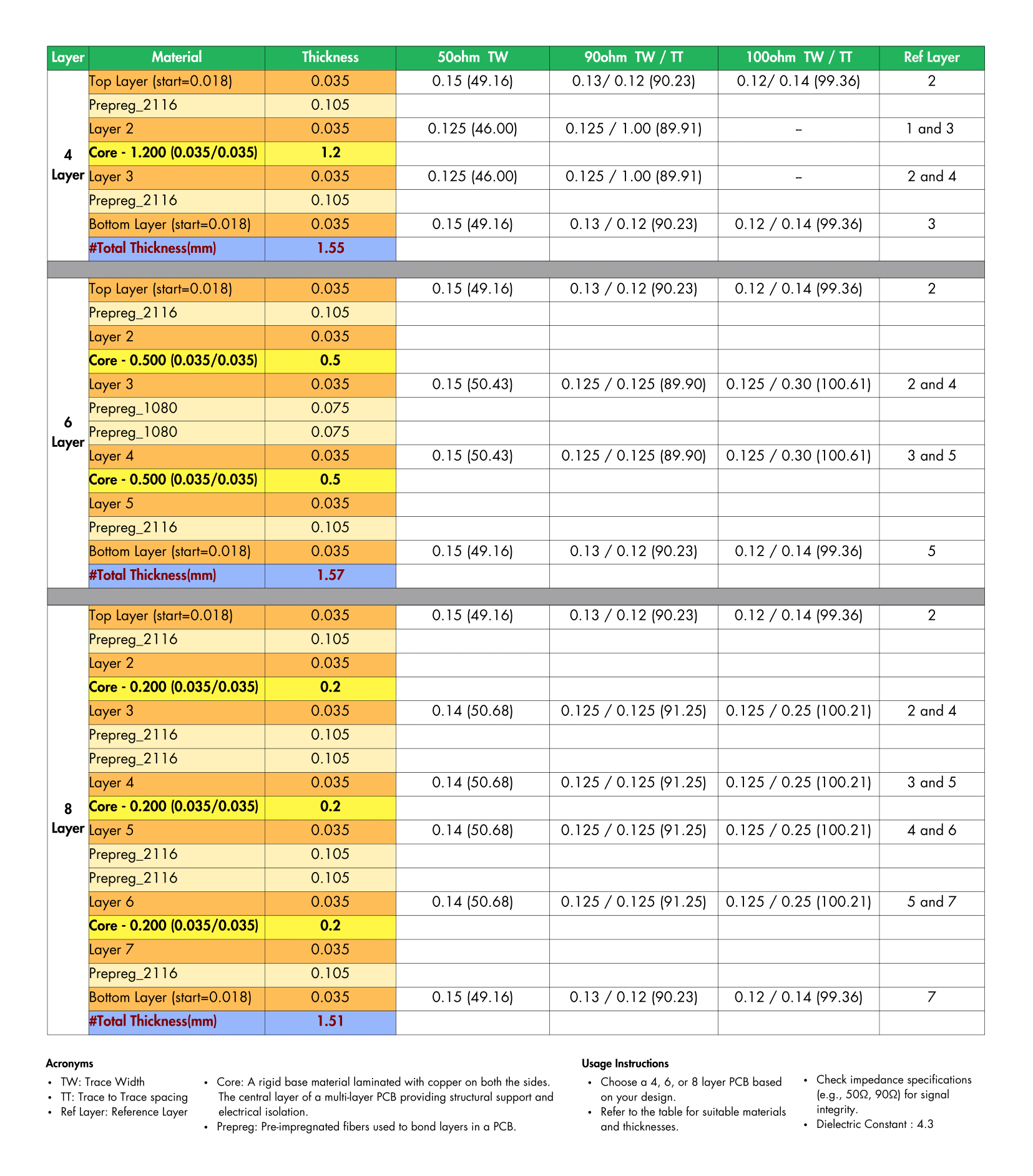
Below are comprehensive details of our 4, 6, and 8-layer impedance-controlled stackups. Each layout specifies exact layer materials, thicknesses, trace widths (TW), and trace-to-trace spacings (TT) engineered to meet target impedance values such as 50Ω, 90Ω, and 100Ω. These specifications are vital for preserving signal quality and performance in high-frequency PCB systems.
Place your order with pcbxpress.
We hope this information provides valuable insights into designing PCB stack-ups that meet your project's unique requirements.
If you have any questions or need further assistance with your PCB stack-up design, please don't hesitate to reach out to our experienced support team. We’re here to help you achieve the best possible PCB configuration for your application.